
Eridonia Archives
(GPU) AMD Radeon RX 5700
(Profile updated as of 16/12/2021)
Here it is. The first profile I made in a long time. This time, it is for my lovely new Radeon RX 5700, based on AMD's all-new "Navi" processor, using RDNA graphics architecture. So this is a really important one for Radeon.
(click for full images)
(Picture 1) Navi 10 graphics processor, surrounded by its eight GDDR6 chips. Each one has a capacity of 1 GiB and operates at 14 Gbps memory data rate. Each chip links into the GPU with a 32-bit interface. Navi 10's memory controller thus aggregates to 256-bit and has 448 GB/s of peak memory bandwidth to 8GB of Video Memory.
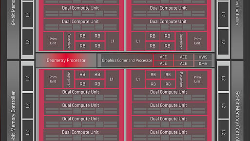
(picture 2) Architectural Block Diagram for Radeon RX 5700's Navi 10 silicon. At the bottom of the diagram you can see two "Dual Compute Units" have been disabled. This reduces the Stream processor and texturing unit count on this video card for binning purposes.
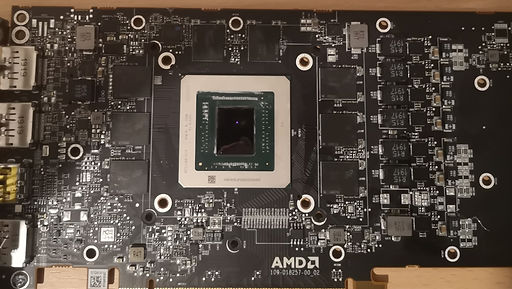
(picture 3) Actual infrared die shot of the Navi 10 XL processor featured in RX 5700. Note the two disabled Workgroup processors; each WGP contains two CU, which contain 64 SP and 4 TMU each. The total compliment of disabled resources for this video card is 256 Stream processorss and 16 Texture Mapping Units.

Graphics Card Information
Graphics Card: AMD Radeon RX 5700
Graphics Card Manufacturer: Advanced Micro Devices
Graphics Card Release Date: July 7, 2019
Graphics Card MSRP: $349 USD
Graphics Processor Codename: "Navi 10"
Graphics Processor Manufacturer: Advanced Micro Devices
Graphics Processor Implementation: Cut die
Graphics Interface: PCI-E 16x Gen4
Architecture: RDNA1
Lithography Process: TSMC 7nm (N7) FinFET
Approximate die size: 251mm²
Sasha's GPU die Size Rating: small
Approximate Transistor Count: 10,300 Million
Approximate Transistor Density: 41 Million / Square Milimetre
GPU Features
Double-speed FP16 Shading: Yes (Rapid Packed Math)
Asynchronous Compute Capability: Full
DirectX Hardware Support: DX12.1 (FL 12_1)
Dedicated DXR Acceleration on chip: No
Variable-rate Shading: No
Adv. Geometry shading: Yes (Primitive Shader Triangle Culling)
Adv. Geometry shading (Programmable/DX12 Mesh Shaders): No
AI/ML Acceleration: No
Advanced Memory Management: No
Integer and Float Shader Co-execution: No
Tile-based Renderer: No
GPU Computing Resources
GPU Substructures: 2 Shader Engines, 18 Workgroup Processors (20 Full Chip)
Graphics Cores: 36 Compute Units (40 Full Chip)
Graphics Cores per Substructure: 1 Shader engine with 10, 1 Shader engine with 8, each Workgroup Processor contains two Compute Units
Total Stream Processors (ALU/Shaders): 2304 (2560 Full Chip)
Stream Processors per Graphics Core: 64
Graphics Core SIMD Structure: 2 x 32
Total Special Execution Units: 72 Scalar Units (80 Full Chip) *
Special Execution Units per Graphics Core: 2 Scalar Units per Compute Unit, 4 per Workgroup Processor *
Total Texturing Units: 144 (160 Full Chip)
Texturing Units per Graphics Core: 4 (Texture filter)
Pixel Pipelines (ROPs): 64 (16 x Render Backend with 4 Pixels per clock)
Level 2 shared on-chip cache: 4096 KB
Geometry/Tessellation Processors: 1 Geometry Engine, 4 Primitive Units (Including Tessellation)
Raster Engines: 4 Primitive Units (Including Rasterisation)
GPU Memory Subsystem
Graphics Memory Type: GDDR6
Graphics Memory Standard Capacity: 8192 MB
Graphics Memory Composition: 8 x 1024 MB GDDR6 DRAM chips
Graphics Memory Access Granularity: 32-bit (4 bytes)
Graphics Memory Standard Clock Speed / Data Rate: 1750 MHz / 14000 MHz
Graphics Memory Full Interface Width: 256-bit (32 bytes per clock)
Graphics Memory Peak Memory Bandwidth: 448 GB/s
GPU Frequency and Peak performance
Graphics Engine Clock: 1725 MHz *
GPU Computing Power FP16: 15,897,600 Million operations per second (FMA)
GPU Computing Power FP32: 7,948,800 Million operations per second (FMA)
GPU Computing Power FP64: 496,800 Million operations per second (FMA)
GPU Texturing Rate INT8: 248,400 Million Texels per second
GPU Texturing Rate FP16: 248,400 Million Texels per second
GPU Pixel Rate: 110,400 Million Pixels per second
GPU Primitive Rate: 6,900 Million triangles per second rasterised (out). 13,800 Million triangles per second into the pipeline before Hardware culling (in). *
GPU Thermal and Power
Standard Cooling Solution: Blower with full-contact copper plate and vapour chamber
Typical Board Power: 180 W
Maximum Board Power: 216 W
Standard External Power Connectors: 6 + 8 pin
Maximum Allowed Junction Temperature (TJ Max): 105*C
Graphics Card description
Radeon RX 5700 is the second-tier product in AMD's new 5700 series lineup, released in July, 2019. It is second to the flagship RX 5700 XT, and differs from that model by having two Workgroup Processors (Dual Compute Units) disabled, losing 256 stream processors and 16 Texture units. The GPU also features a lower power target of 180W, versus the ~200W limit on RX 5700 XT. In addition, the non XT model has a smoother shroud compared to the stylised version on the XT.
This graphics card's processor, known as "Navi 10", is based on the all-new "RDNA" architecture. This architecture is set to replace the aging Graphics Core Next architecture, which is in its 5th iteration, with the "Vega" series of silicon. "RDNA" and "Navi" introduce some very significant changes to the GPU Shader cores, I typed some bits on the RDNA architecture, here and here. Essentially, RDNA has a much lower instruction latency, as the GPU now natively works with groups of 32 threads (instead of 64 for GCN) and each of these groups can be completed in one clock cycle. This allows the Compute Unit to accept a new group of threads/instructions every clock cycle, where it took 4 cycles on previous GCN designs. The direct result, is RDNA-based graphics processors can achieve signficiantly higher shader utilisation in video gaming and 3D workloads; as you will notice these cards have far fewer Stream processors compared to Vega-based models, but acheive the same or higher performance.
AMD has made significant improvements to performance per watt, and utilising TSMC's 7nm 'N7' lithography, Radeon RX 5700 can match the energy efficiency of Nvidia's latest cards, something Radeon hasn't been able to do in nearly a decade.
Navi implements a functional 'Primitive Shader' system that was first marketed as functioning on 'Vega' based processors. While the implementation on Vega failed to yield any significant improvement to performance (whether this is due to issues in-silicon is unknown), "Navi" based silicon can cull triangles at an extremely high rate, in hardware. The "Navi 10" processor in the RX 5700 can accept up to 8 triangles into the graphics pipeline, and use Primitive Shading methods to cull 50% of them, and finally draw 4 to the screen. This is likely an advanced progression of the "Primitive Discard Accelerator" introduced in Polaris. Essentially, this allows the GPU to very quickly throw away triangles that are not visible (and thus would waste GPU rasterisation time, adding frame latency and reducing the Frame rate for no reason). Navi 10 appears to have some quirks with pure Tessellation synthetics, it is important to note that the Geometry processor is likely to have been entirely re-distributed to optimised transistors and die area to gaming workloads. It is not a good idea to take pure synthetics as real-world performance traits, but you can read about that here.
Also of note, is "Navi 10" silicon, as featured in the Radeon RX 5700 graphics card, is the first consumer graphics processor to feature support for the PCI-e 4.0 standard. Actual gaming benefits are this time are marginal to non-existent, but certain I/O reliant compute workloads can see major advantages.
It is important to note that the RX 5700 doesn't feature any support for DXR or Hardware Ray Tracing currently, AMD's driver doesn't expose the code paths to allow DXR to function on the shader array as of publishing of this profile. Like all DX12 compliant GPUs, the 5700 can Ray Trace on its shaders, but without any (advertised) hardware capable of accelerating it, NVidia's 20-series will offer vastly higher performance in this use case. However, the Radeon RX 5700 is not marketed towards Ray Tracing, and is offered as a compelling alternative to those gamers who do not want to pay the premium for Ray Tracing currently.
Graphics Card approximate 3D Performance
Sasha's gaming performance rating (2019): Great for 1080p High Refresh (144 Hz) or 1440p 60 Hz gaming with maximum settings
The Radeon RX 5700 provides performance roughly similar to Nvidia's RTX 2070 (non Super) and RTX 2060 Super graphics cards. It is not-insignificantly faster than its price counterpart, the RTX 2060 (non Super) and also provides 8GB of VRAM, instead of 6 on that card. As a result, performance is greater than the fabled GTX 1080 of 2016, by about 10-15%. Power consumption is about the same, or a bit lower than that card, so energy efficiency is slightly higher. As a result, this card is capable of driving a 1920x1080 monitor with all graphics settings dialed up (without Ray Tracing), and high framerates, well over 100 FPS in most titles. The card is aimed at providing capable 2560x1440 gaming performance at 60 Hz and above, where it performs well.
Notes
Tile-based Renderer:
I am currently unsure of the nature of the Draw-Stream Binning Rasteriser in Navi silicon. I am fairly certain it does feature some form of Tile-based renderer, however.
Special Execution Units:
I am currently unsure of the amount of Load/Store Units in the CU for Navi. I think it remains the same as GCN, at 16, but I will not list them here until I have solid confirmation, as the new block diagrams for Navi don't actually state LSUs at all.
Graphics Engine Clock:
As with "Vega" based cards, this represents the hard-limited maximum clock speed for the graphics processor. Actual, in-game clock speed will be slightly lower, depending on many factors such as thermals, power use and I assume, silicon quality. It is important to note that "Navi 10" introduces a new "Game clock" rating that will be more realistic of the speeds you will see in 3D, gaming workloads. That speed is 1625 MHz. In my experience with the RX 5700, actual clock speed is closer to 1700 MHz, even under full load.
GPU Primitive Rate:
This is based on my understanding of Navi's Primitive Shading implementation for fast hardware culling.
Architecture:
AMD doesn't officially classify this silicon as 'RDNA1' but as it will likely receive architectural revisions and updates, much like GCN before it, I will call "Navi 10" "RDNA1", or "1st Generation RDNA".
Misc.
This bit is for my personal opinion on this Graphics card / Graphics processor
Sasha's Awesomeness Rating: Cool.