
Eridonia Archives
(GPU) AMD Radeon RX Vega 64
(profile updated as of 16/12/2021)
My Hardware profile for AMD's return to the high end in 2017, the Radeon RX Vega 64 graphics card. I actually owned two of these cards, one Reference Liquid Edition, and one Powercolor Red Devil. The pictures here are from the Red Devil (my friend took them for me before he sold the card to me) as I never took my Liquid Edition apart.
(click for full images).
(picture 1) Vega 64: Vega 10 GPU package. This is the unmolded version, where the HBM stacks (the two smaller chips) are not surrounded by an epoxy mould to strengthen them. Each stack consists of 4x 1GB DRAM chips 3D stacked on top of each other, and on a Logic die, then connected to the GPU via the interposer with 1024 lanes(bus width). Vega 10's two stacks give it a 2048-bit wide memory interface.
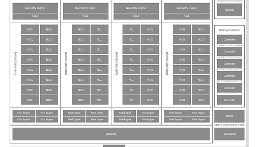
(picture 2) Architectural block diagram for Vega 64.
(Picture 3) Actual silicon die shot for Vega 10 GPU as featured in the Vega 64. Image credit: Fritzchens Fritz


Graphics Card Information
Graphics Card: AMD Radeon RX Vega 64
Graphics Card Manufacturer: Advanced Micro Devices
Graphics Card Release Date: August 14, 2017
Graphics Card MSRP: $499 USD
Graphics Processor Codename: "Vega 10 XT"
Graphics Processor Manufacturer: Advanced Micro Devices
Graphics Processor Implementation: Full Chip
Graphics Interface: PCI-E 16x Gen3
Architecture: Graphics Core Next 5th Generation (GCN5)
Lithography Process: Global Foundries 14nm (LPP) FinFET
Approximate die size: 495mm² *
Sasha's GPU die Size Rating: Large
Approximate Transistor Count: 12,500 Million
Approximate Transistor Density: 25 Million / Square Milimetre
GPU Features
Double-speed FP16 Shading: Yes (Rapid Packed Math)
Asynchronous Compute Capability: Full
DirectX Hardware Support: DX12.1 (FL 12_1)
Dedicated DXR Acelleration on chip: No
Variable-rate Shading: No
Adv. Geometry shading: No (Preliminary)
Adv. Geometry shading (Programmable/DX12 Mesh Shaders): No
AI/ML Acceleration: No
Advanced Memory Management: Yes (HBCC)
Integer and Float Shader Co-execution: No
Tile-based Renderer: No (Preliminary)
GPU Computing Resources
GPU Substructures: 4 Shader Engines
Graphics Cores: 64 Compute Units
Graphics Cores per Substructure: 16
Total Stream Processors (ALU/Shaders): 4096
Stream Processors per Graphics Core: 64
Graphics Core SIMD Structure: 4 x 16
Total Special Execution Units: 64 Scalar Units, 1024 Load/Store Units, 64 branch Units
Special Execution Units per Graphics Core: 1 Scalar, 1 Branch, 16 Load/Store Units
Total Texturing Units: 256
Texturing Units per Graphics Core: 4
Pixel Pipelines (ROPs): 64 (16 x Render Backend with 4 Pixels per clock)
Level 2 shared on-chip cache: 4096 KB
Geometry/Tessellation Processors: 4
Raster Engines: 4
GPU Memory Subsystem
Graphics Memory Type: HBM2
Graphics Memory Standard Capacity: 8192 MB
Graphics Memory Composition: 2 x 4-high stacks (4x 1024 MB DRAM dies each stack)
Graphics Memory Access Granularity: 1024-bit (128 bytes)
Graphics Memory Standard Clock Speed / Data Rate: 945 MHz / 1890 MHz
Graphics Memory Full Interface Width: 2048-bit (256 bytes per clock)
Graphics Memory Peak Memory Bandwidth: 483.8 GB/s
GPU Frequency and Peak performance
Graphics Engine Clock: 1546 MHz *
GPU Computing Power FP16: 25,329,664 Million operations per second (FMA)
GPU Computing Power FP32: 12,664,832 Million operations per second (FMA)
GPU Computing Power FP64: 791,552 Million operations per second (FMA) (1:16 FP32)
GPU Texturing Rate INT8: 395,776 Million Texels per second
GPU Texturing Rate FP16: 197,888 Million Texels per second
GPU Pixel Rate: 98,944 Million Pixels per second
GPU Primitive Rate: 6,184 Million triangles per second
GPU Thermal and Power
Standard Cooling Solution: Triple-fan open-air with Vapor Chamber Heatsink
Typical Board Power: 295 W
Maximum Board Power: - *
Maximum Allowed Junction Temperature (TJ Max): 100*C
Graphics Card description
Radeon RX Vega 64 marked AMD's return to high-end GPUs after 2016's Polaris architecture was entirely for the mid-range with the flagship RX 480 offering performance similar to NVIDIA's GTX 1060 6GB. The RX Vega 64 uses the full implementation of the "Vega 10" silicon, featuring the 5th iteration of the Graphics Core Next architecture. Vega brings new technologies such as Rapid Packed Math (double-speed Half-precision shading) and an advanced memory management system called HBCC (High-Bandwidth Cache Controller), which essentially uses paging methods to manage GPU accesses to system RAM, potentially smoothing out framerate spikes when the card runs out of dedicated HBM2 VRAM, by allowing the GPU to use that 8GB as a "cache".
Vega architecture also introduced a new method of handing geometry, AMD calling it "Next Generation Geometry Fast Path" or "Primitive Shaders". These would allow the GPU to cull triangles extremely quickly by merging Vertex and Geometry Shaders together into a new "primitive shader". For unknown reasons this technology is not fully featured on Vega-based GPUs, or doesn't actually provide increased performance over the normal Geometry pipeline. (See Notes). Vega's Render backends are directly linked into its relatively large L2 cache, at 4096KB. This allows them to offload render work directly into the huge bandwidth provided by the cache, then onto the HBM2 when necessary. This change helps Vega achieve higher performance with less bandwidth than Fiji-based cards. The other major change of GCN5 was optimisation for much higher clock rates than previous designs: over 1.5 GHz is possible on "Vega 10" silicon.
Vega-based GPUs also advertised a type of "Tiled Renderer" known by AMD as the "Draw Stream Binning Rasteriser". This this feature appears primarily to reduce bandwidth reliance and power consumption in certain scenarios, by splitting the frame into "bins" and rendering sequentially which reduces memory requirements by limiting the size of the workload. The time taken to draw the frame remains similar to drawing the entire frame at once, but reduces the memory footprint, in my understanding. As far as I know, DSBR is not functional on Vega 10; the framebuffer colour data is drawn in full directly from the dedicated VRAM after spilling out of L2 cache.
RX Vega 64 is AMD's first GPU to use High Bandwidth Memory 2nd Generation (HBM2) which it employs a dual-stack design for a bus-width of 2048-bits and 4-high stacks on the consumer cards giving it a total of 8 GB of graphics memory on package. The HBM2 frequency target was missed (2 Gbps) and as a result the Vega 10 silicon actually has less bandwidth than its predecessor, Fiji, at only 483 GB/s versus 512 on that GPU.
Graphics Card approximate 3D Performance
Sasha's gaming performance rating (2019): Great for 1440p gaming maximum settings
Radeon RX Vega 64 was likely supposed to target the GeForce GTX 1080 Ti 's performance (That was released shortly before). For various reasons the GPU was unable to provide performance on average similar to the GTX 1080 Ti, and instead competed directly with the incumbent GTX 1080, but uses significantly more power. In 2019 it hasn't gained a lot of performance but now beats out the GTX 1080 in many games more often than it did before. As a result it provides performance similar to the RTX 2060, actually sitting between that card and the more powerful RTX 2070, and depending on the game, can actually match the latter. This makes the card great for 1440p gaming or high refresh 1080p gaming. You can also play 4K with normal/high settings at playable framerates.
Notes
Adv. Geometry shading (Primitive/Mesh shaders):
Vega-based GPUs were advertised as being able to utilise a new "Fast Path" geometry system at the shader-level, but in my understanding, it is not fully functional / implemented / beneficial on Vega graphics processors.
Graphics Engine Clock:
Vega-based cards utilise a dynamic boosting algorithm, similar in functionality to NVIDIA's "GPU Boost" feature. The stated clock speed is AMD-spec maximum boost clock speed. Actual gaming frequency will vary a bit based on many factors such as temperature, power limits etc.
Tile-based Renderer:
Vega-based GPUs feature what AMD calls "Draw-Stream Binning Rasteriser". This is, in effect, a type of tile-based renderer, however to my knowledge it is not fully enabled in all games on the desktop Vega-based cards. In Vega, this feature is primarily used to reduce memory bandwidth requirements and power consumption, rather than improve performance significantly. It is, as a result, more useful on the Vega-based integrated Graphics processors featuring on the "Raven Ridge" Silicon.
Approximate die size
Actual stated die size measurement for this Graphics Processor varies a bit. AMD's official number on launch was 486 square millimetres as tweeted by Raja Koduri, however in later slides comparing to Vega 20; it is listed as 495. Fritzchen Fritz has measured the die size during the die shot process to be just under 510 square millimetres. The discrepancy is likely to do with measuring the internal logic die and the package within which the processor is contained. I am listing 495 as it is the latest measurement from official AMD material as far as I know.
Maximum Board Power:
I am currently unsure of the maximum board power allowed on reference Vega 64 cards. Maximum within PCI-E spec is 375W (75+150+150).
Misc.
This bit is for my personal opinion on this Graphics card / Graphics processor
Sasha's Awesomeness Rating: Awesome